I. Concept & Participants Diagram
A. Concept
B. Mission
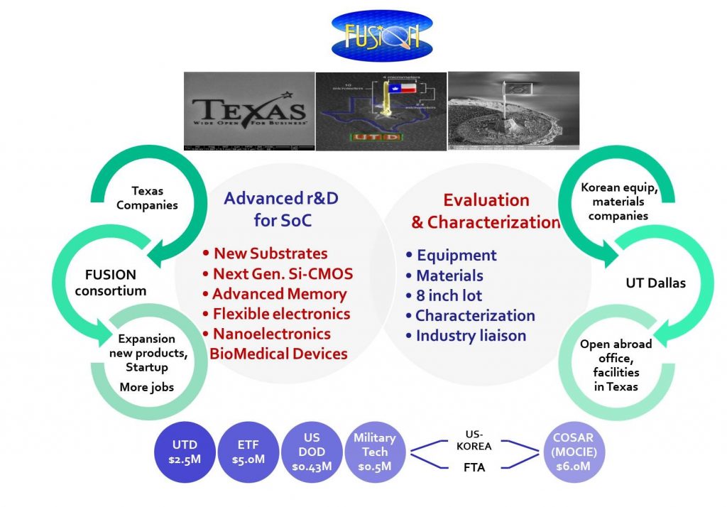
The proposed new Texas FUture Semicondcutor CommercializatION (Texas FUSION) program will expedite the commercialization of products by actively transferring technology and information to consortium member companies, forming new startup companies for unique products, and attracting companies to set up their headquarters or branch offices in Texas.
C. Research Activity & Research Team
A team of recognized experts in the field of semiconductor technology, flexible electronics, nanoelectronics, biomedical applications, RF and high speed sensor for defense applications and low power circuits will combine and coordinate expertise to successfully execute the proposed research. With applied R&D as the main focus, the proposed research will support critical technology development that will lead to unique product scenarios: (i) low-power electronics based on novel nanoelectronics for medical and defense applications, (ii) high-power, high-speed RF electronics for defense applications, (iii) flexible electronics for defense and entertainment applications, and (iv) large scale non-volatile embedded memory.
D. Advisory Board
The FUSION Advisory Board shall be composed of selected individuals with extensive applicable experience in strategic development and management of technology development and commercialization programs or corporate entities. It shall, in general, be responsible for advising the FUSION Program Manager on strategic and management issues; and have primary responsibility for fostering activities to accelerate the commercial application of research results produced by the FUSION program.
SEE MORE DETAILS
E. TETF Members
-Academia Industry
-UT Dallas Texas Instruments
-UT Austin TriQuint Semiconductor
-UT Southwestern Medical Center
-UT Tyler Samsung Austin Semiconductor
-UT Arlington Military Tech
-IntelliEpi
-Kairos Microsystems Corporation
-Syzygy Memory Plastics
F. KETI Diagram
II. Programs Based on Funding
1. TETF: State of Texas Emerging Technology Fund
Research Projects (2009 ~ 2013)
| UT Tyler | David Crook | “For Fabrication of a Biocompatible Conformal Strain Sensor” |
| UT Southwestern Medical Center | Jinming Gao & Baran Sumer | “Dual MRI/Fluorescent Nanoprobes for Robotic Surgery of H&N Tumors” |
| UT Dallas & Syzygy Memory Plastics | Walter Voit | “High Channel Count, Shape Memory Polymer, Carbon Nanotube Electrodes in Degradable Drug-Eluting Hydrogels as Reliable Central Nervous System Interfaces” |
| UT Dallas & KMC | Kenneth O, D. Ma and J. Brewer | “RF Circuits – Shielded Inductors for Mitigation of Effects of Surrounding, Monolithic 3V-Input Switched-Capacitor Power Converter on 65nm CMOS” |
| UT Arlington | Sung yong Jung | “Development of an Adapter Board and a Smart Phone App for the Microneedle Based Non-Enzymatic Glucose Sensor” |
| UT Dallas | J.B. Lee | “Microneedles for transdermal drug delivery and neural interface applications” |
| UT Austin | Jack Lee | “High-K III-V Semiconductor MOSFETs” |
| UT Dallas | W. Duncan | “Ischemia Detection During Surgery Using Raman Spectroscopy” |
| UT Dallas | Manuel Quevedo | “Development of Large Area Neutron Detectors Based on Organic Solid State Detectors Fabricated on Flexible Substrate” |
| UT Dallas | Moon Kim | “Heterogeneous Integration for Multi-functional Devices” |
2. KETI : Korea Electronics Technology Institute Fund
Research Projects (2008-2012)
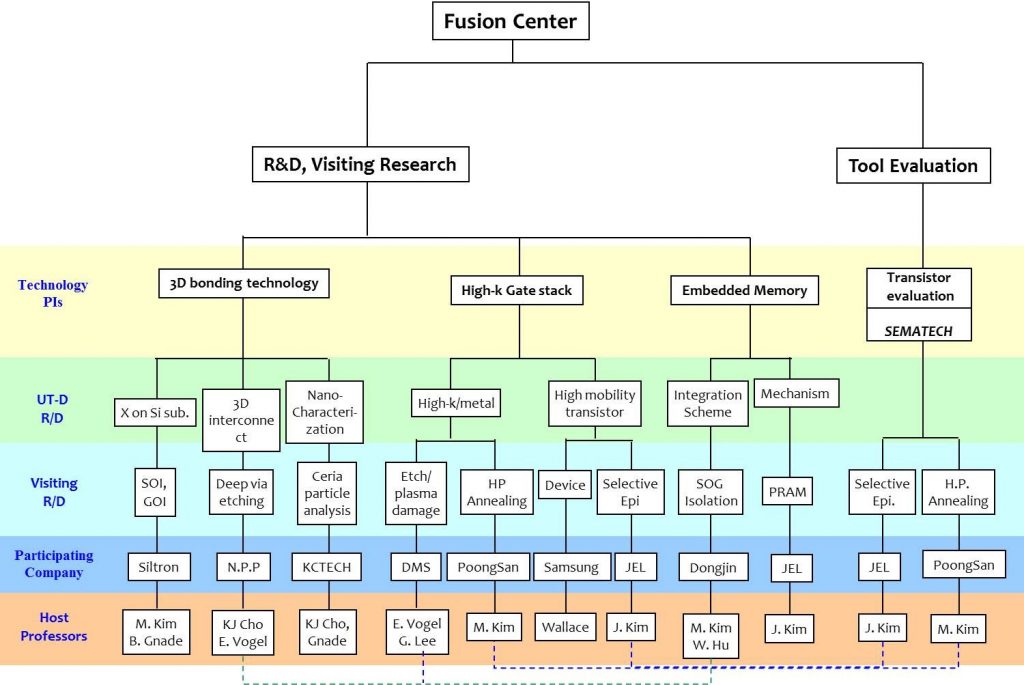
| DMS | “Development of Next Generation High Density Plasma Etcher” |
| DMS | “Development of in situ surface analysis technology for semiconductor processing” |
| DONGJIN SEMICHEM Co., Ltd | “Nano-scale selective multilayer deposition technology using atomic layer deposition (ALD) and self-assembled monolayers (SAM)” |
| DONGJIN SEMICHEM Co., Ltd | “Development of next generation Spin-on-dielectric (SOD) Material” |
| NCD Technology | “Development of atomic layer deposition system for next generation electronic device” |
| New Power Plasma Co., Ltd | “22nm fine pattern fabrication technology” |
| K.C.Tech Co., Ltd | “Development of Low Resistivity TiN ALD Process & Cu Seed Technologies” |
| Samsung Electronics Co., Ltd | “Development of Gate dielectric for the application of design rule (DR) under 20nm” |
| Korea Electronics Technology Institute | “Research of next generation semiconductor technology trend and commercialization” |
| Jusung Engineering Co., Ltd | “Development low cost, low defect a-Si:H/Si/SiGe/Ge tandem solar cell” |
| New Power Plasma | “Deep via etch process development & process kit optimization” |
| SNTEK Co., Ltd | “Application and evaluation of a nano-scale damageless etch system to next generation semiconductor devices” |